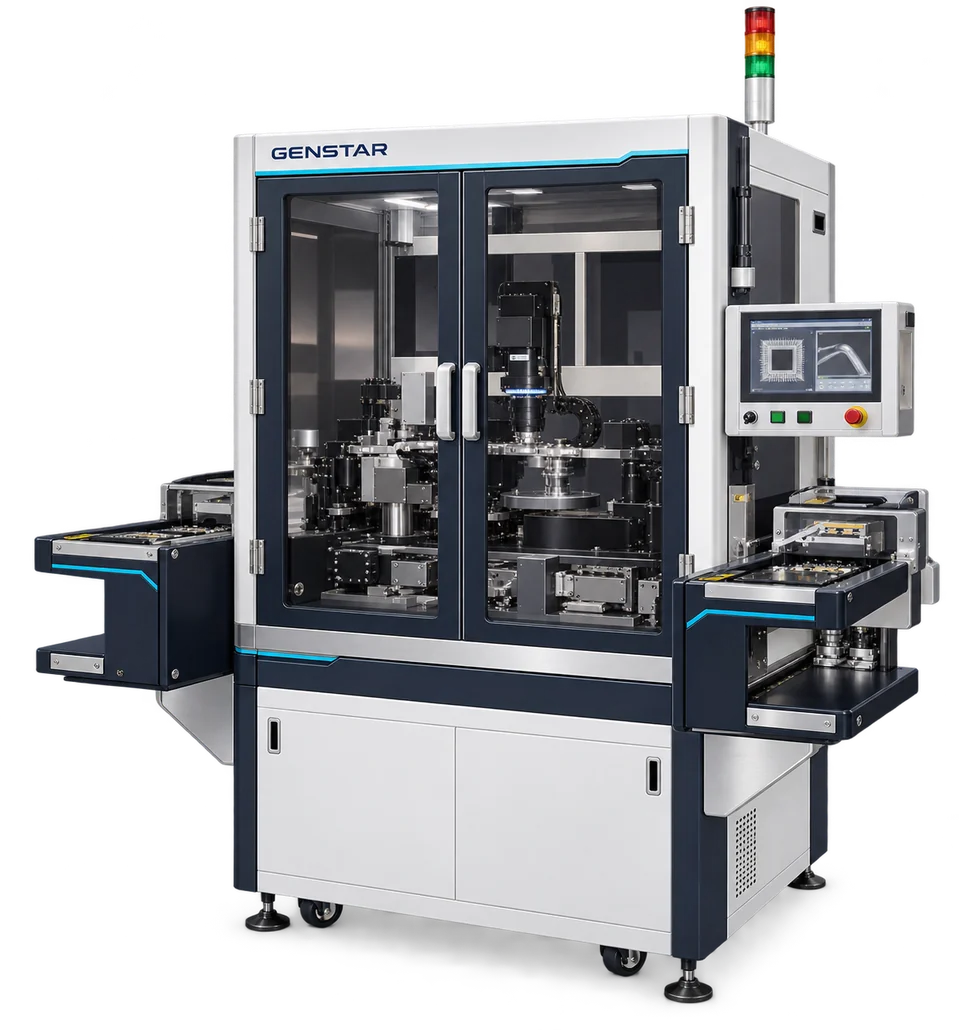
WireBond 2D / 3D inspection system
2D visual and 3D optical inspection for semiconductor packaging, covering ICs, capacitors, silver plating, lead frames, wires and bonds.
Explore product

PRODUCTS & SOLUTIONS
Find products and solutions by application or inspection technology.
EXPLORE OUR PORTFOLIO
13 items
2D visual and 3D optical inspection for semiconductor packaging, covering ICs, capacitors, silver plating, lead frames, wires and bonds.
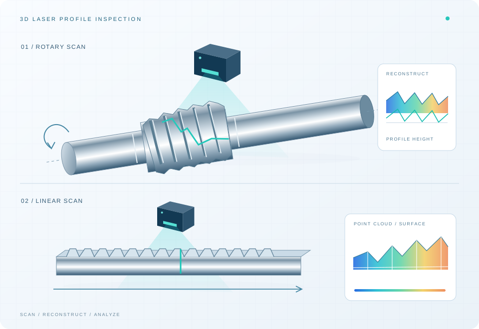
Inspect wear and structural abnormalities in automotive steering shafts and racks after durability or impact testing.
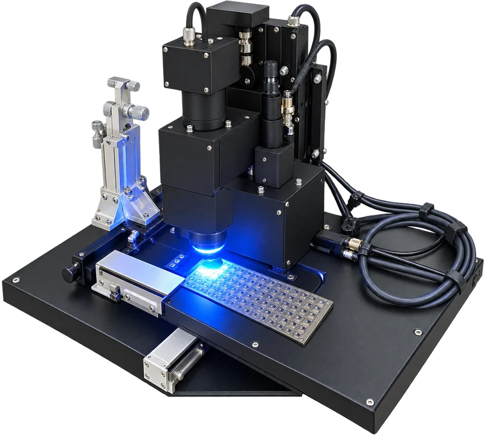
Manually load and position samples, then use microscope focus-based measurement to inspect WireBond loop height, bond geometry and position.
Inspect wire shape, loop height and bond positions in power devices.
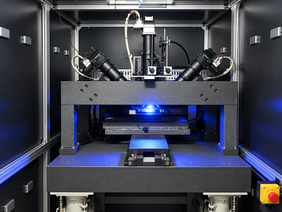
Measure microbump diameter, height and 3D shape.
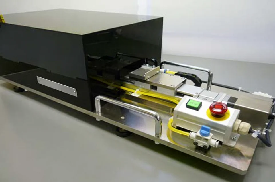
A manual solder-bump inspection system for package and flip-chip substrates, measuring coplanarity and inspecting tip profiles and attached foreign material.
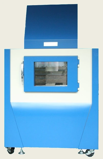
Use a sealed microfocus X-ray source for internal radiographic observation and sample evaluation.
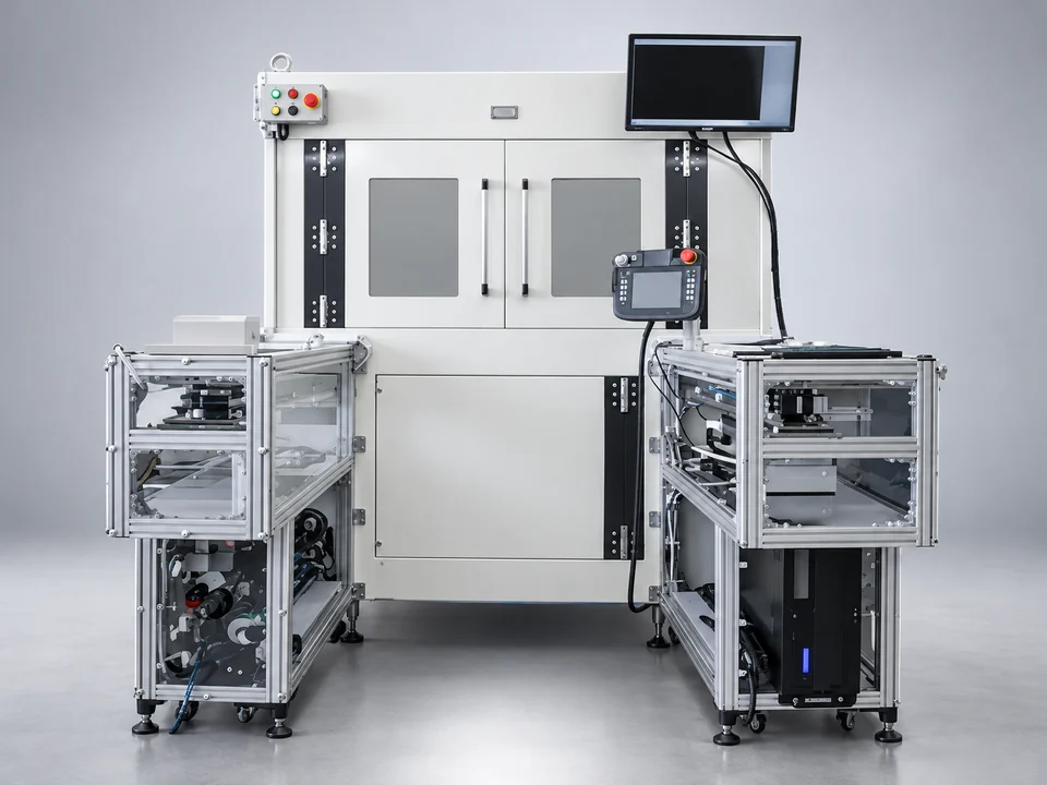
Combine X-ray radiography, feeding, handling and reject processing for packaged devices.
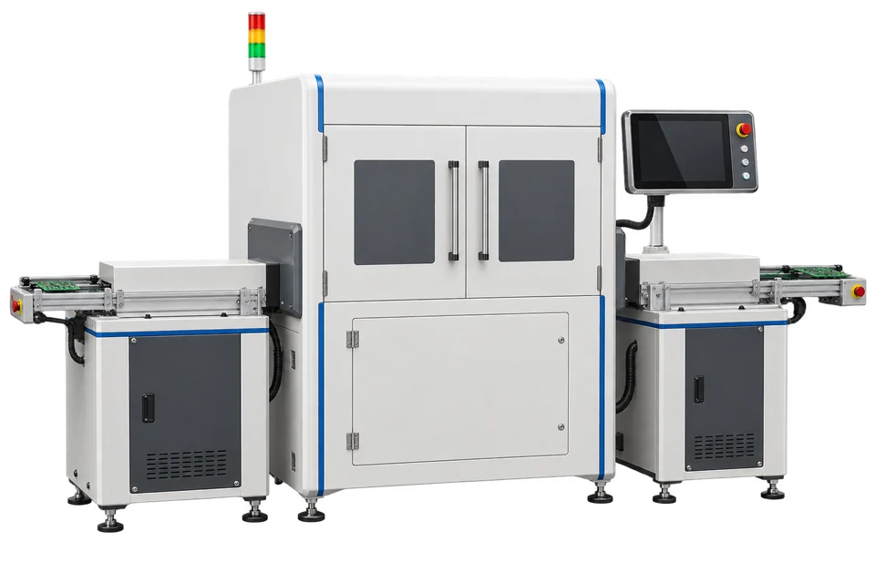
Combine X-ray radiography with conveyor handling to inspect PCBs and assembled boards. Configure imaging and automation around board construction, inspection areas and production flow.
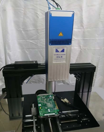
Use chromatic confocal measurement for steps, protrusions, scratches and film thickness.
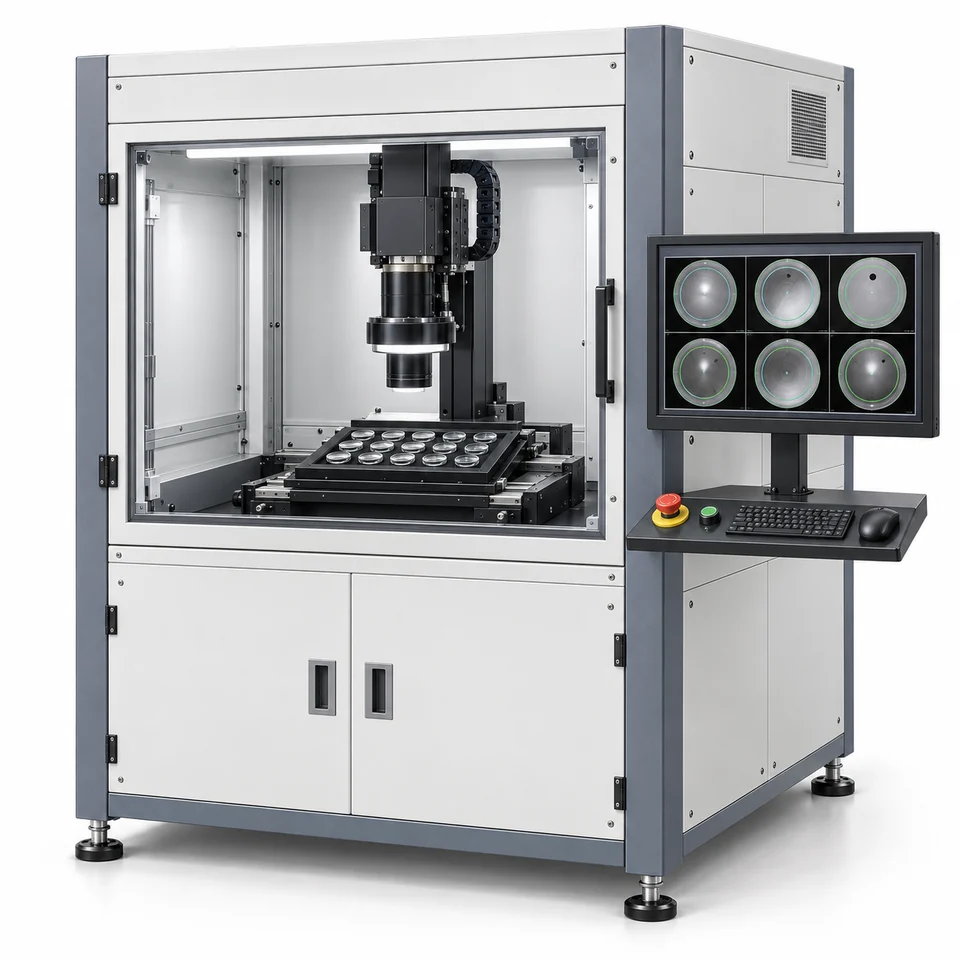
Inspect glass lenses on trays using dedicated illumination and image processing.
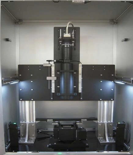
Combine dedicated optics, a line-scan camera and positioning for pin-gauge inspection.

Enterprise data, reporting and natural-language queries
LET'S CONNECT
Get in touch for an initial enquiry, a technical conversation or a discussion of possible solutions.